Integrated circuits are fabricated using planar technology on single crystalline semiconducting substrates. The substrate, called a wafer, is shaped as a disc typically 50 - 300mm in diameter and less than 1mm thick. On one wafer from tens to hundreds of individual ICs were fabricated.
Planar technology is based on the deposition or growing of conductive and dielectric layers, transfer of the desired pattern into that layers and doping of parts of substrate with specific impurities. The loop above is repeated continously depending on the complexity of the device. Layers as thin as a few atoms up to a thickness of some micrometer are made. The lateral dimensions created by modern lithography and etching are below 180nm in the most advanced devices in mass production. In typical submicron silicon technology around one third of the several hundred manufacturing steps are based on plasma processing. The subsequent formation of conductive lines for wiring and dielectric layers for vertical isolation, with small openings to connect the different wiring levels, leads to a complicated topography on the device, imposing significant challenges to the structuring process.
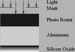
Figure ![[*]](crossref.png) shows a typical sequence to
form an aluminum interconnect layer. First the aluminum is
deposited by a sputter process; next the light sensitive
photo-resist is coated on the metal by a spin-on process.
The photo-resist is then exposed through a mask
with light of a suitable
wavelength1.1. This light
changes the chemical structure of the resist,
making it soluble in a suitable liquid, by a process is called
development. The total resist coating, exposure and
development sequence is named lithography. After replicating
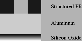
the mask pattern into the resist the transfer to the
aluminum by etching takes place.
In modern processes plasma etching is applied as it
best keeps the sizing of the resist mask which protects
the material at the desired locations from being etched.
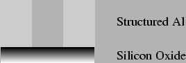
Finally the remaining photo-resist is removed by dissolving
it in a liquid or transforming it to volatile species
that can be pumped away in a vacuum chamber. The later
process is usually done in a plasma assisted environment
and called plasma stripping or ashing.
shows a typical sequence to
form an aluminum interconnect layer. First the aluminum is
deposited by a sputter process; next the light sensitive
photo-resist is coated on the metal by a spin-on process.
The photo-resist is then exposed through a mask
with light of a suitable
wavelength1.1. This light
changes the chemical structure of the resist,
making it soluble in a suitable liquid, by a process is called
development. The total resist coating, exposure and
development sequence is named lithography. After replicating
the mask pattern into the resist the transfer to the
aluminum by etching takes place.
In modern processes plasma etching is applied as it
best keeps the sizing of the resist mask which protects
the material at the desired locations from being etched.
Finally the remaining photo-resist is removed by dissolving
it in a liquid or transforming it to volatile species
that can be pumped away in a vacuum chamber. The later
process is usually done in a plasma assisted environment
and called plasma stripping or ashing.
The other main task in semiconductor manufacturing, beside the delineation of designed patterns, is the doping of specific areas on the device. Hereby it is possible to alter the conductivity of silicon by many orders of magnitude and nonlinear effects appear which allow to create electronic devices. Doping is done in a similar manner as the structure formation described above. First the mask that covers the areas which should not be processed is created by lithography. Then a ion beam built of species to be implanted is directed towards the wafer. Depending on the energy of the particles and the exposure time of the wafer to the beam, different depth profiles can be achieved. In silicon technology mainly boron, phosphorus or arsenic is used to form the n and p regions necessary to build field-effect and bipolar transistors.
back to www.gs68.de
Other important things: Legal Notice, Contact us
Copyright © 2001-2012 Spitzlsperger Technologies GmbH